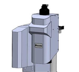
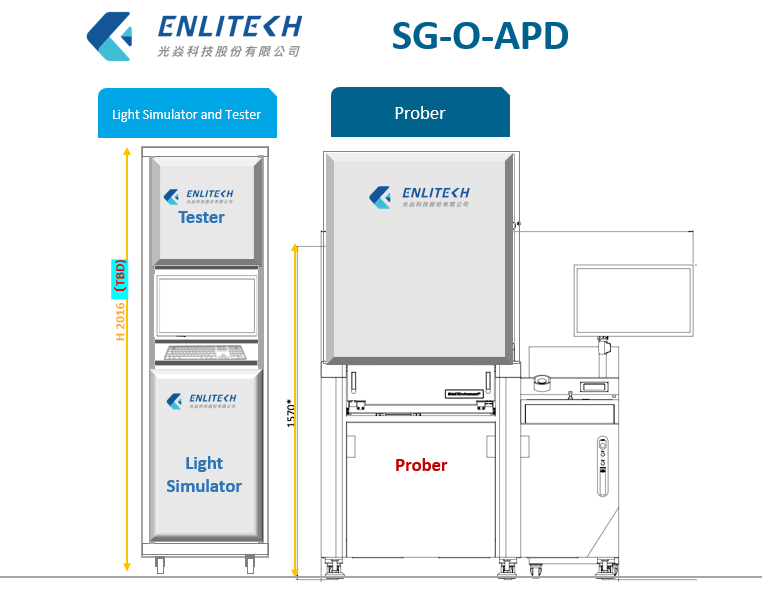
Description
Provide All You Need in CIS / ALS / Light-Sensor Wafer Level Testing.
- “6S” Commercial wafer grading inspection models:
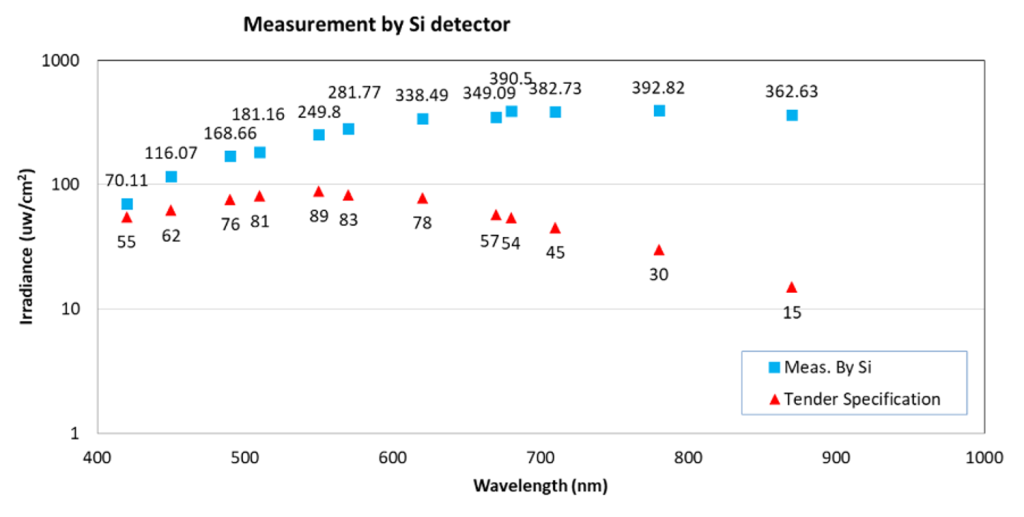
- Super-Wide (Wide Spectral Range from UV to SWIR)
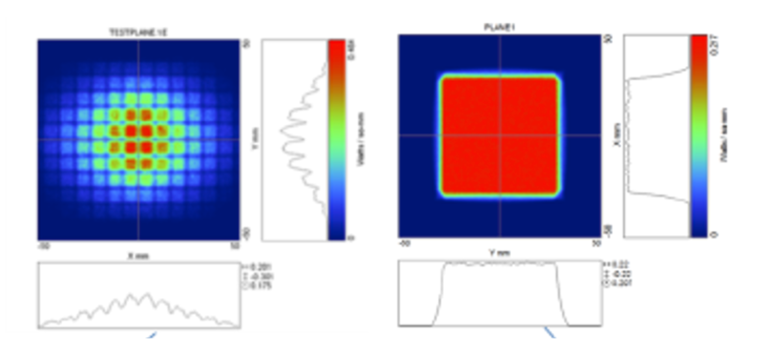
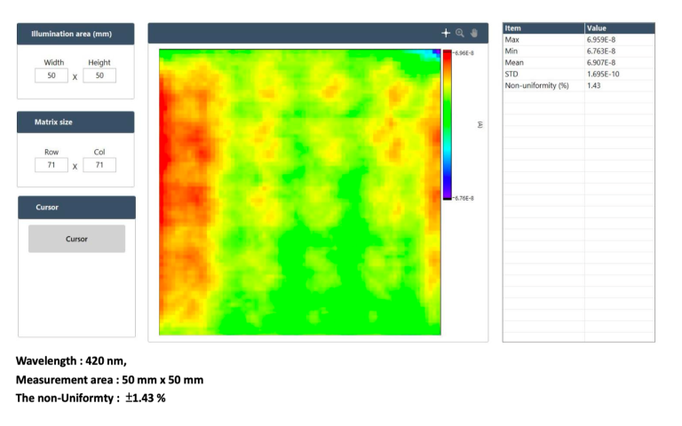
- Super-Uniformity (Uniformity Better Than 98% Over 50mm x 50mm Area)
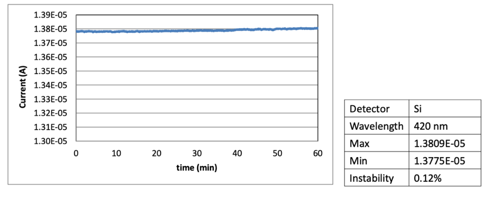
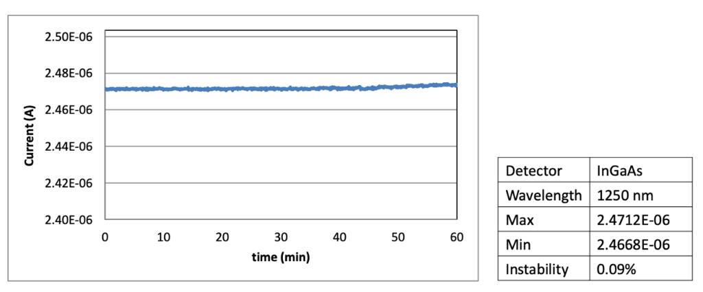
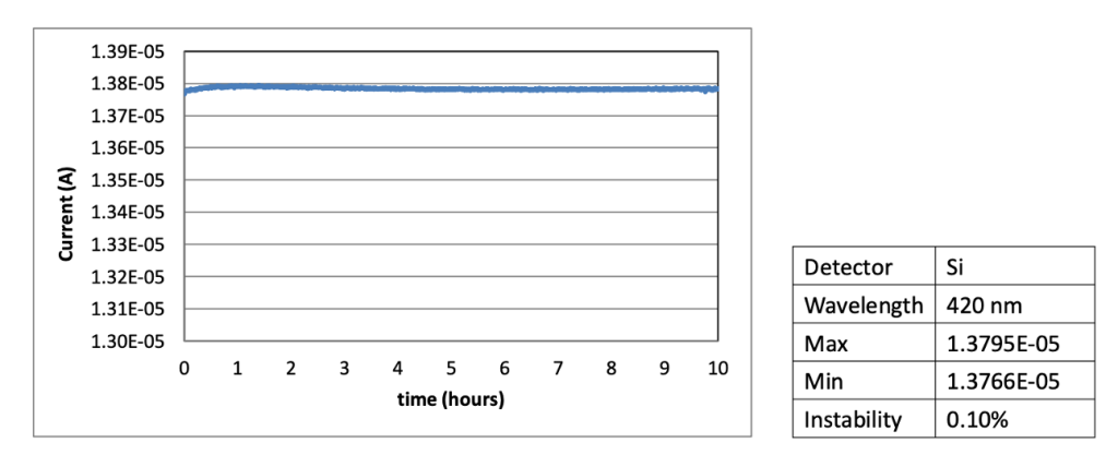
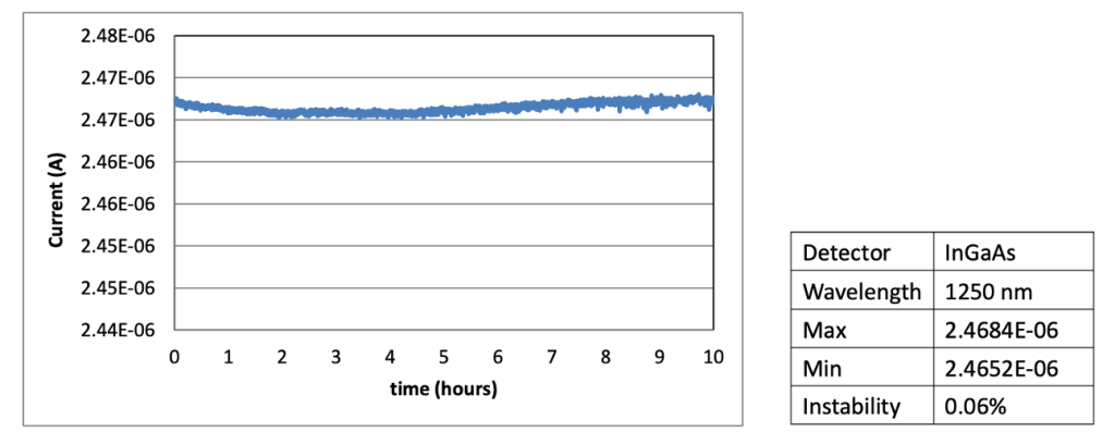
- Super-Stable (Stable Light Intensity In-stability < 0.2% over 10hrs)
- Super-Wide (Wide Range of Temperature from -80°C to 180°C)
- Super-Low(Ultra-Low Noise for Accurate CIS / ALS / Light-Senser Wafer Testing)
- The first commercially available image sensor wafer tester with EMVA1288 grading.
- The only choice for wafer-level CIS efficiency testing, eliminating the need for self-construction and reducing measurement inaccuracies.
- High integration with automation and semi-automation equipment, providing high flexibility
- (Automatic wafer loading machine, modular chuck)
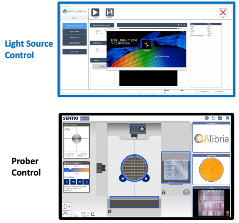
- Integrated software
- Streamlined operations and accelerated development speed
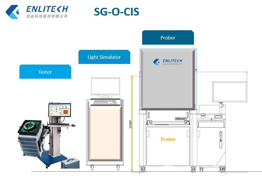
- Complete product line
- Enlitech offers a complete product line that includes the SG-A and SG-O series. These products are designed to be used with the same infrastructure, allowing seamless integration from upstream to downstream processes.
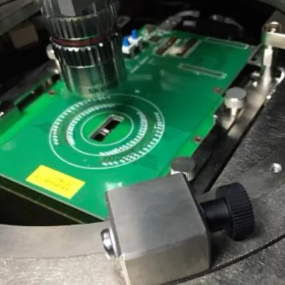
- Programmable automated detectors
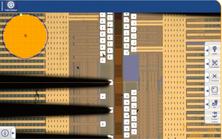
- Capable of handling 200mm wafer size and single chips larger than 1cm x 1cm
- Highly uniform light source
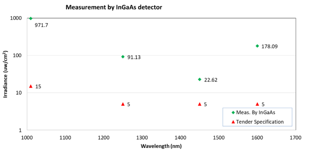
- Capable of providing a continuous white light spectrum ranging from 400nm to 1700nm, as well as monochromatic light output with a certain Full Width at Half Maximum (FWHM) at various specific wavelengths.
- Support for ultra-large wafer and chip sizes
- The detector can handle wafer sizes up to a maximum of 200mm and single chips larger than 1cm x 1cm.
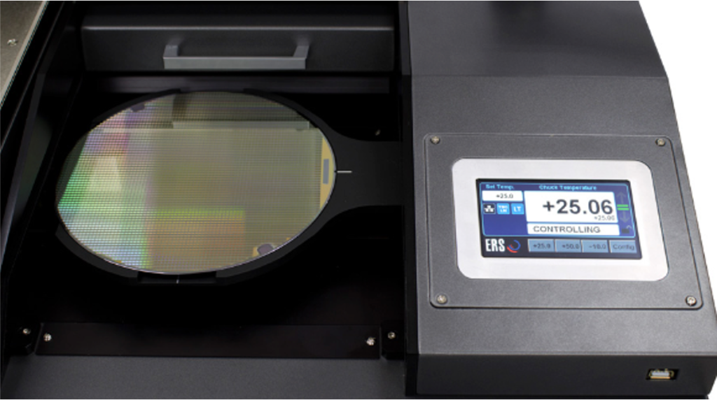
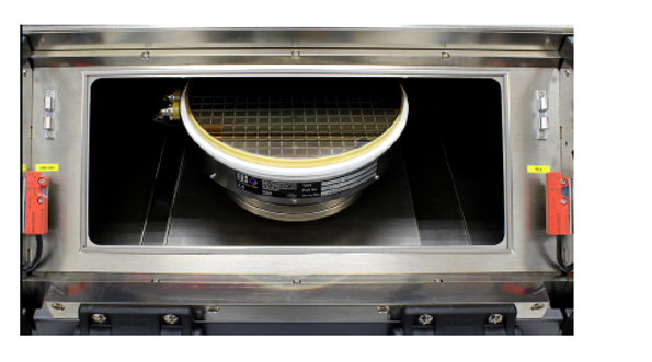
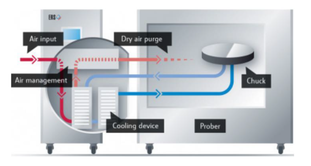
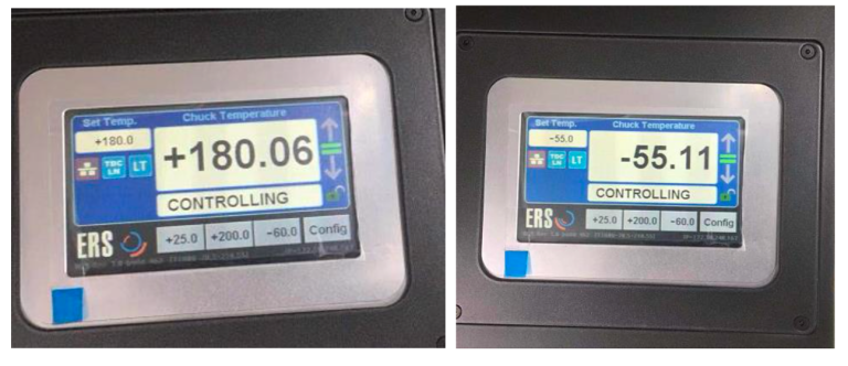
- Low-noise operation at a wide range of temperatures
- Equipped with an ultra-low noise thermal chuck, supporting a temperature range from -60°C to 180°C, with rapid heating rates and stability.
- Integrated equipment and one-stop solutions
- We provide one-stop solutions for your CIS (CMOS Image Sensor), ALS (Ambient Light Sensor), and photodetector design verification or process yield inspection needs.
Features |
||
Highly Uniform Light Source |
Programmable automated detectors | Wide temperature range and low-noise chuck |
| Wide Spectral Range from UV to SWIR | Processing capability for wafer or chips ranging from 200mm to 10mm | Modular chuck |
| High uniformity with over 98% homogeneity across an illumination area exceeding 50mm x 50mm | Used for highly accurate and reliable DC/CV and RF measurements | Wide temperature range of -80°C to 180°C |
| Ultra-stable light intensity, maintaining instability below 0.2% for over 10 hours. | Stable functional microscope system | Advanced CDA (Closed-Loop Direct Air) thermal control technology with high ramp rates and temperature stability at high temperatures. |
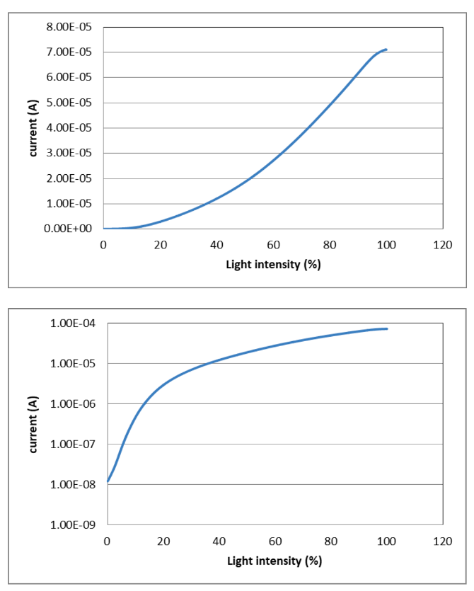
| High dynamic range of light intensity, reaching up to 140dB | Integrated hardware control panel | Ultra-low noise for precise CIS/ALS/photodetector wafer testing |
|
Automatic wafer loading machine
|
||
| Intelligent wafer mapping | ||